Designing PCBs with KiCad
This documents the process of milling a Hello World board for the Fabacademy (part of the electronics design week assignment).
Assignment
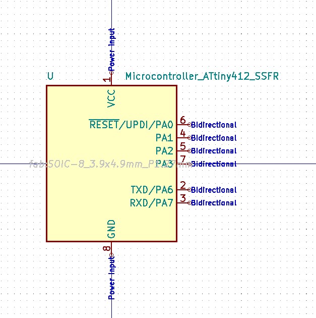
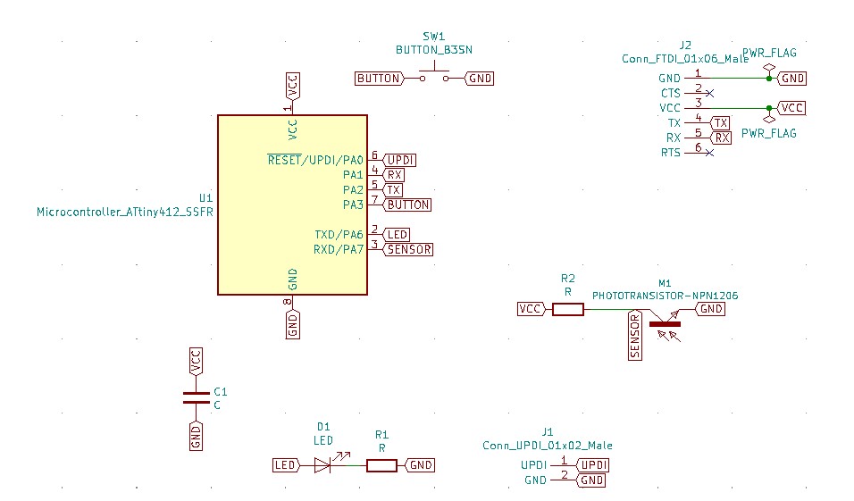
We’re gonna be working with an ATTiny 412 for this project. The components that we’re going to need are:
- ATTiny 412
- Button (tact switch) (SWITCH 6x6mm in the electronics cupboard)
- LED
- Current-limiting resistor
To calculate the current limiting resistor value that you need, you can use https://ledcalculator.net/. (LED: R = (V_source - V_led) / I_led)
- Phototransistor
- UPDI pins
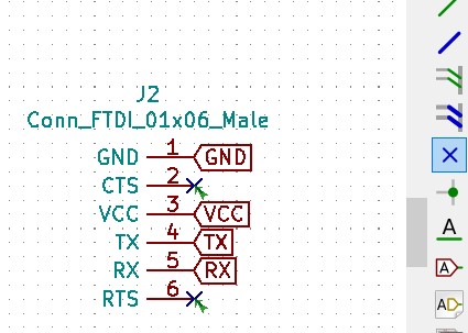
- FTDI pins
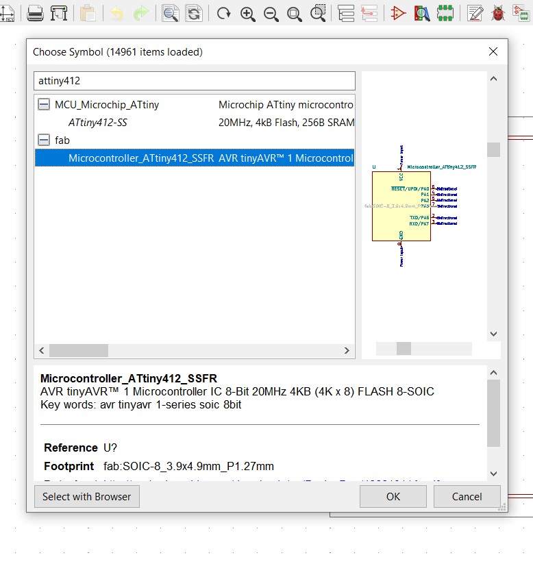
For KiCad, download the fablab library for components. Follow the instructions in the readme to get started with the library.
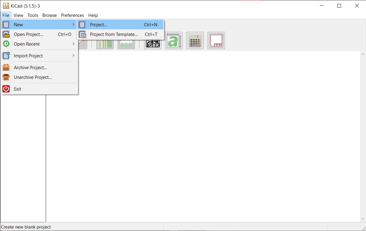
Start a new project:
Then open the schematic layout editor:
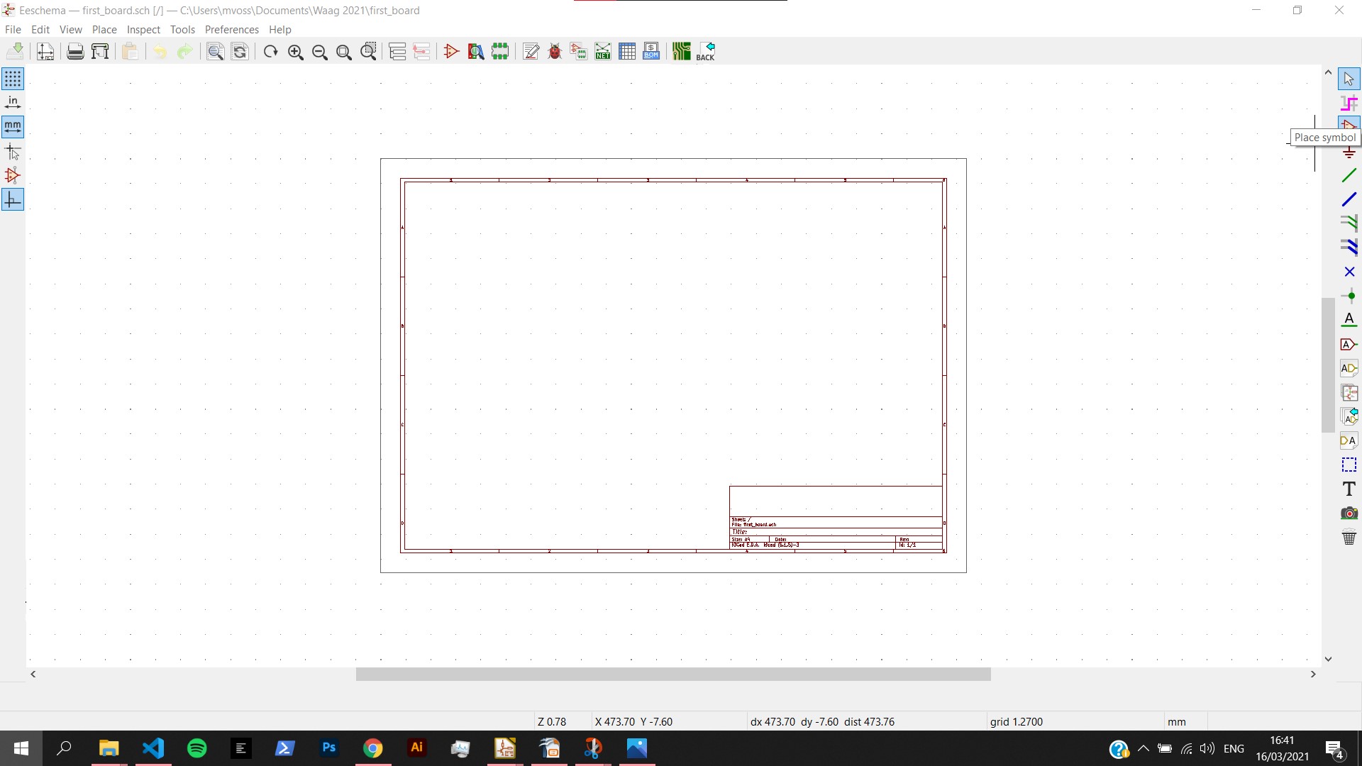
Shortcuts that I used:
- M: move component
- W: place wire (shift + w)
- R: rotate
- C: copy
-
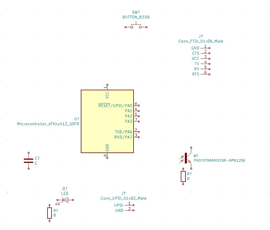
Place components
-
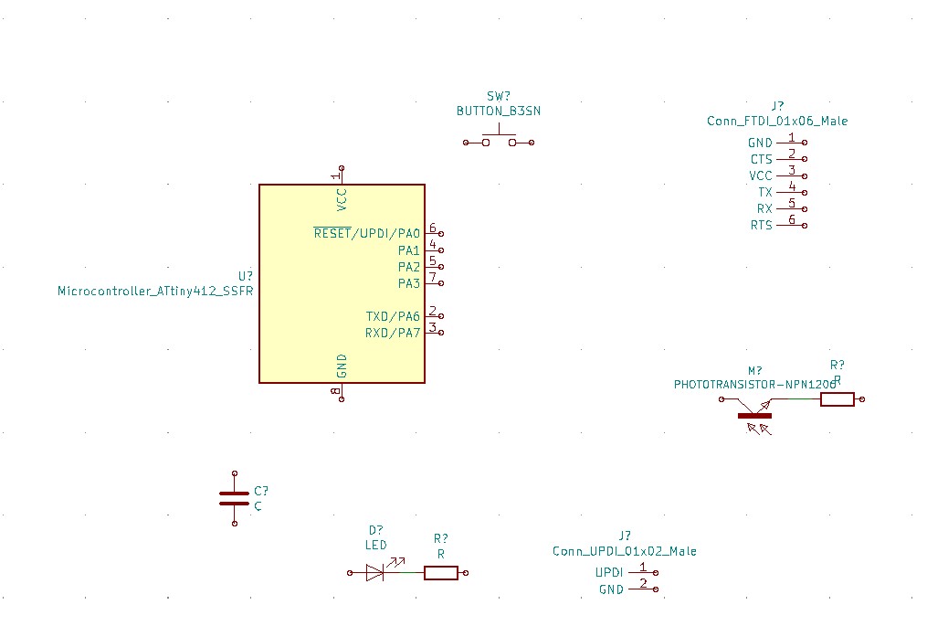
Connect components such as LED’s to resistors using wires
-
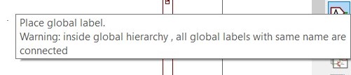
Connect other components using global labels (this connects the labels on different components with each other)
-
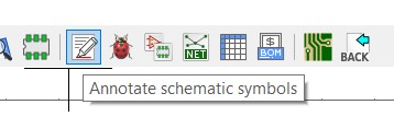
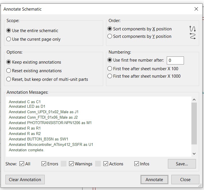
Annotate schematic symbols
-
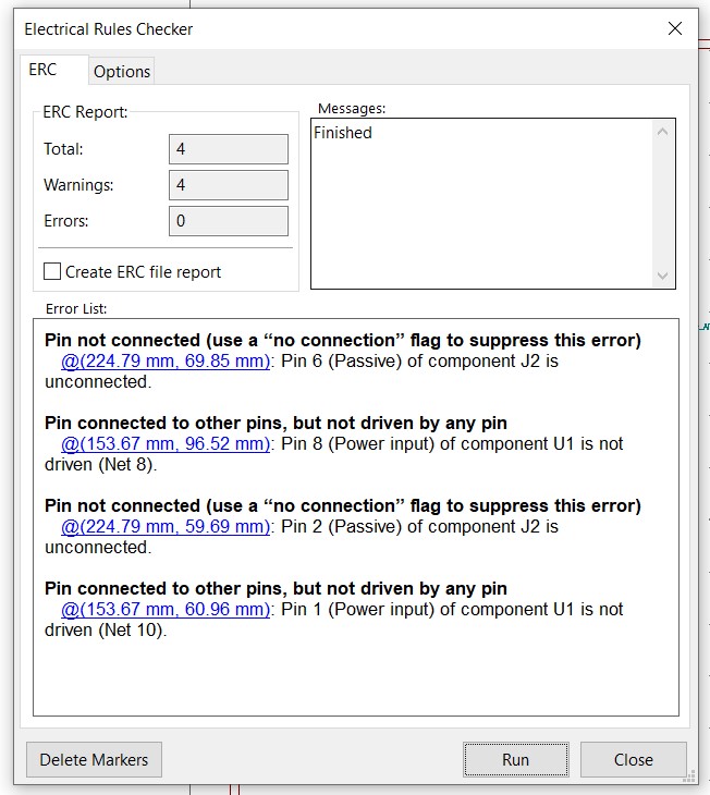
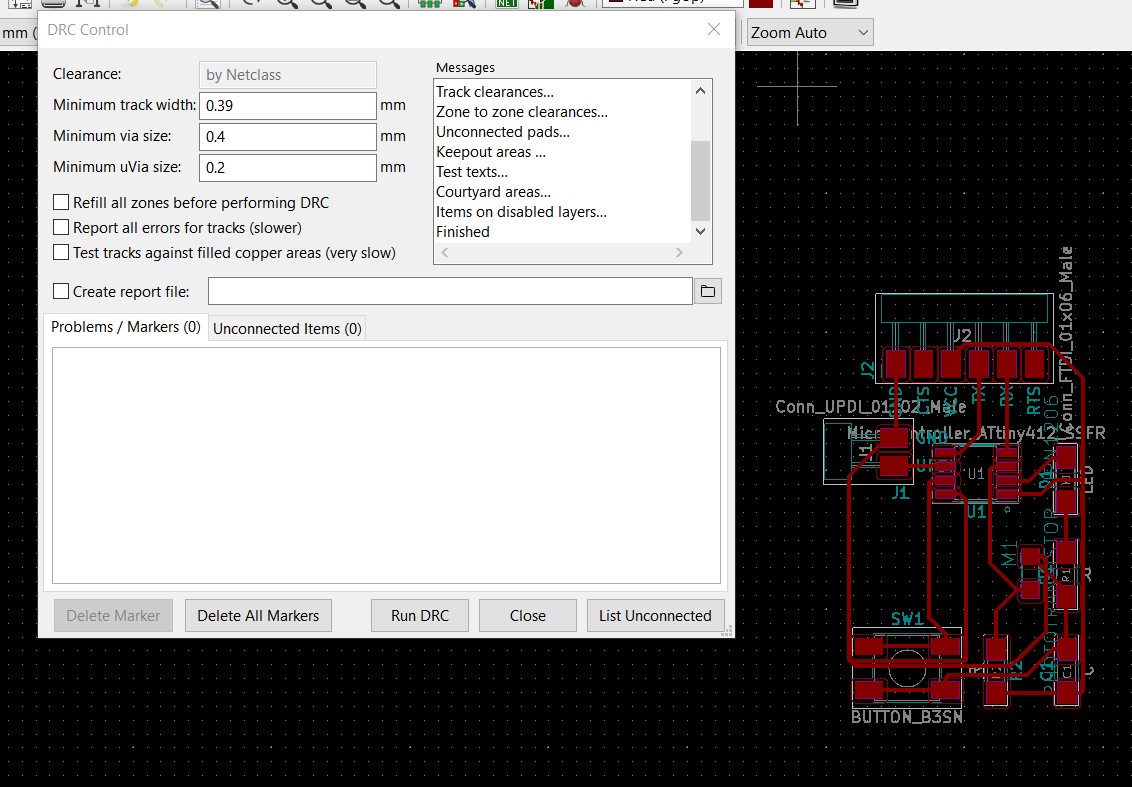
Perform electrical rules check
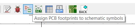
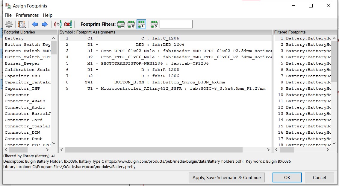
- Assign footprints (to determine the arrangement of the pads for the SMD’s) (don’t forget to press ‘apply, save schematic & continue’)
- Generate netlist
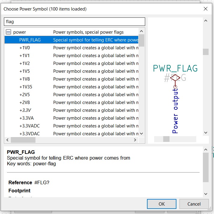
- there’s no power supply because the power will be provided by the FTDI so ignore those warnings or place a power flag

- you can place a no connection flag if you’re not using a pin
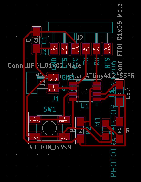
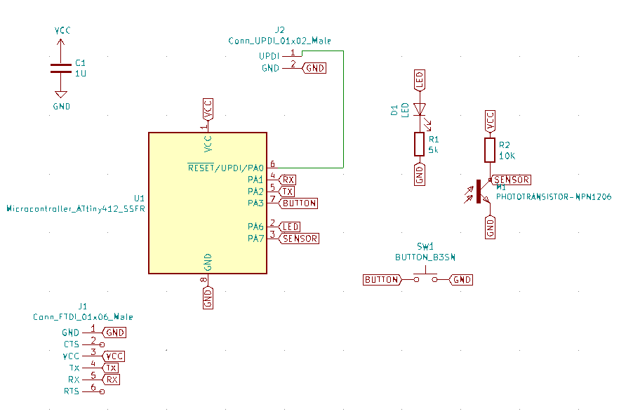
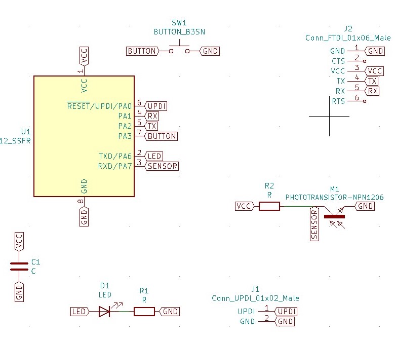
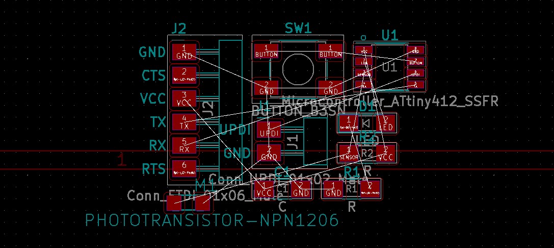
My final schematic looks like this:
Then once you’re done, you can exit the schematic layout editor and return to the Kicad overview. The next step is to create the actual footprints for our board, which we can do in the PCB layout editor.
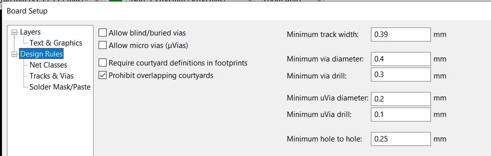
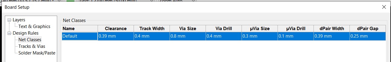
It’s important to specify the design rules (the limits of the milling machine you’re using, so precision and milling bit).
Click on the Board Setup button along the top to open a new window in which to update the design rules of the Roland Modela milling machine (I copied the settings from Nadieh’s documentation).
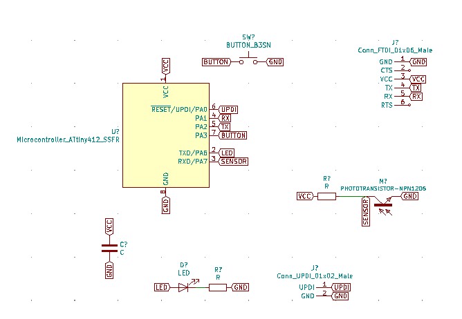
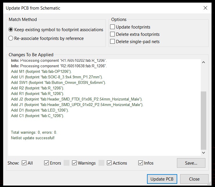
Load the components by clicking update PCB from schematic. Here I encountered the following error:
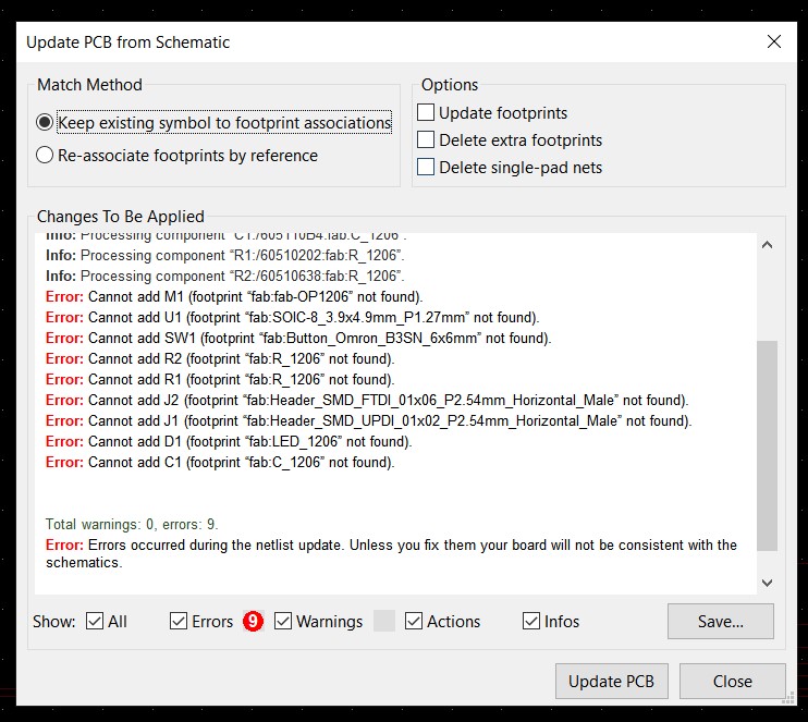
So I returned to the schematic layout editor to see if I could find what went wrong. After running the assign footprints tool and opening one of the components (right click > view component) I ran into this error:
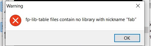
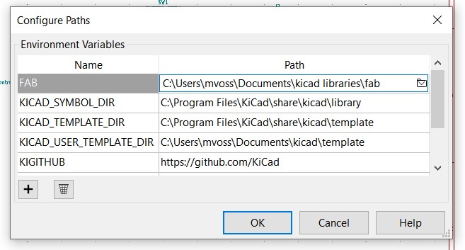
So something went wrong with importing the fab library; after checking the the preferences I noticed that the footprint library wasn’t imported so I redid that. After that the import was succesful and my footprints appeared.
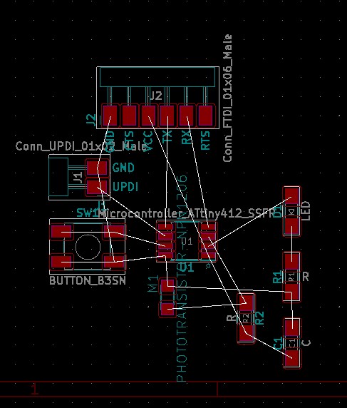
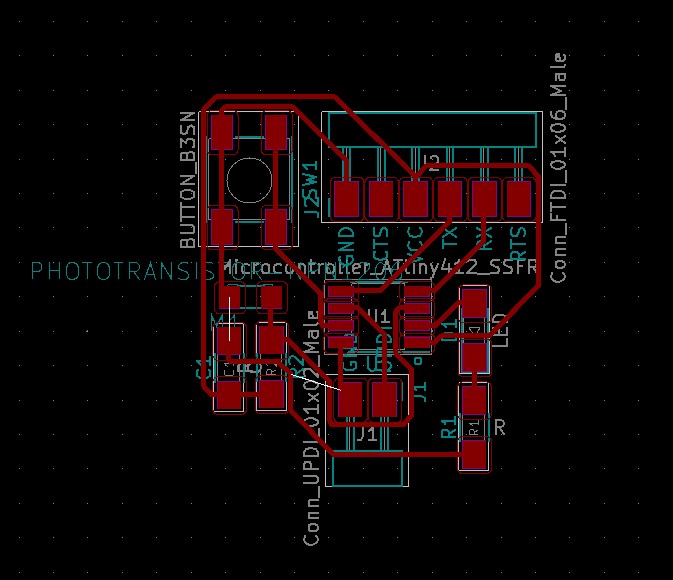
Now it’s time to sort out the rat’s nest (that’s what the components with the tangled air wires is called) that has appeared.
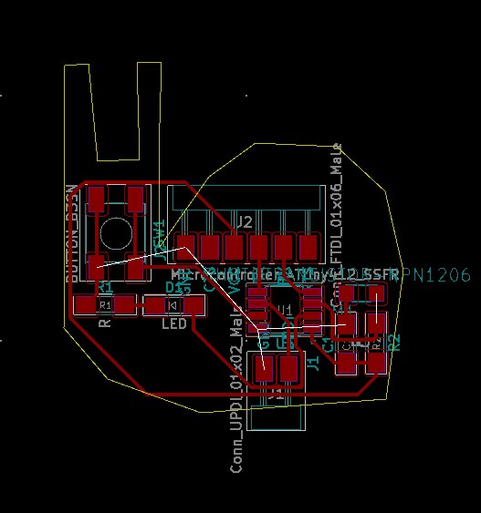
For small boards like this it’s recommended to draw the traces by hand. It’s quite a puzzle since you’re often left with just one trace that’s impossible to draw, but I think it’s fun figuring it out. KiCad prohibits you from crossing traces; if there’s a possibility it will draw a wire for you around the traces you already have (for example using the space underneath components as bridges). Here some attempts:
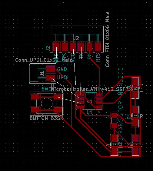
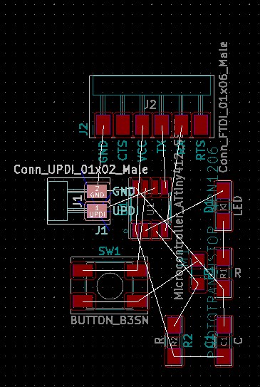
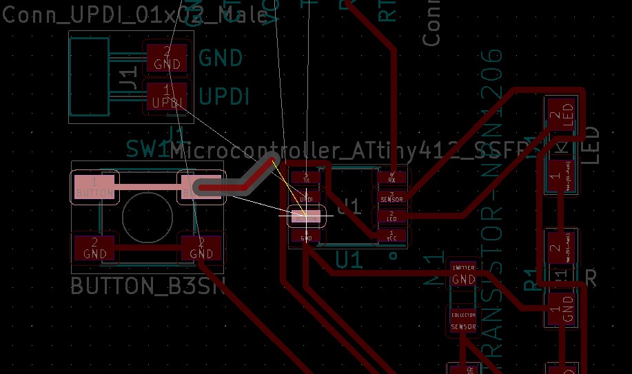
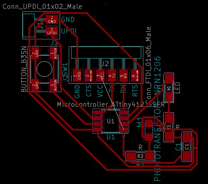
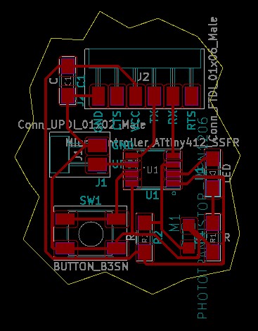
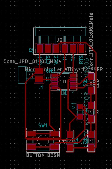
My succesful attempts:
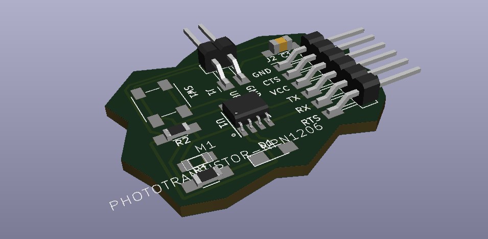
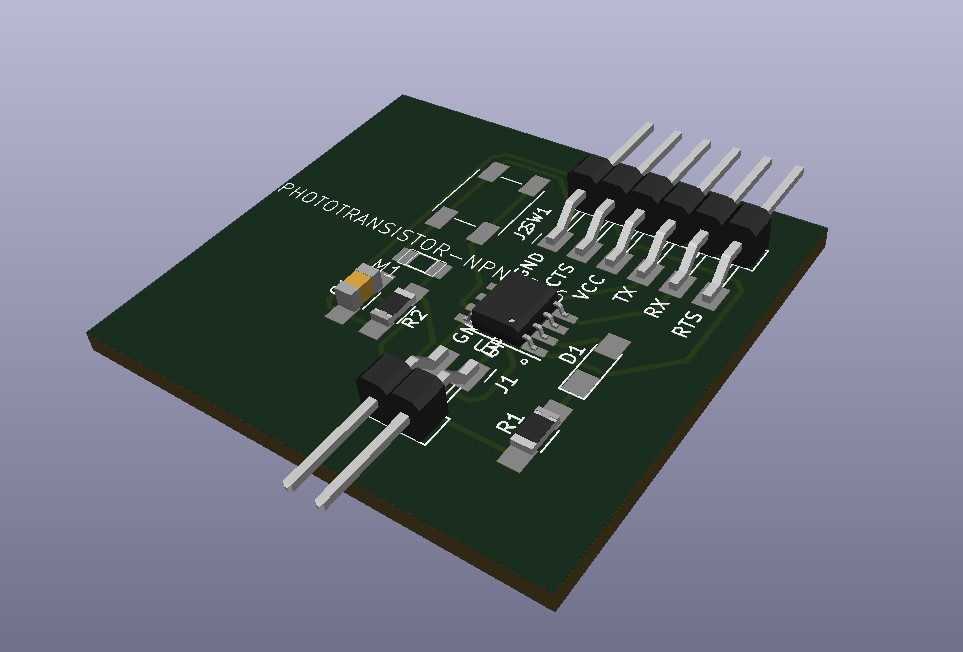
A 3D view of the second PCB:
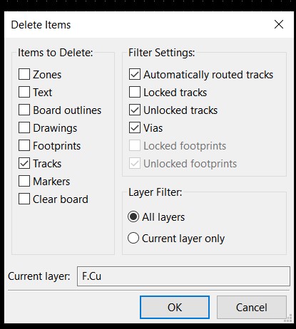
I didn’t quite like the design yet so I continued fiddling a bit more. A good tool to remember is Global Deletions; here you can delete all tracks in one go. If you want to delete a whole track, hover over it and press I > backspace.
After reading through documentation of this assignment I realized I had to connect the ATTiny to the FTDI via the capacitor so I started over again, but this time I first tried defining the edge cut so I had some bounderies to keep in mind for my design. However that really restricts you in your design so it’s easier to do the edge cut last. I went back to my first attempt and made some tweaks (mostly moving the capacitor so it was in between the FTDI and the ATTiny).